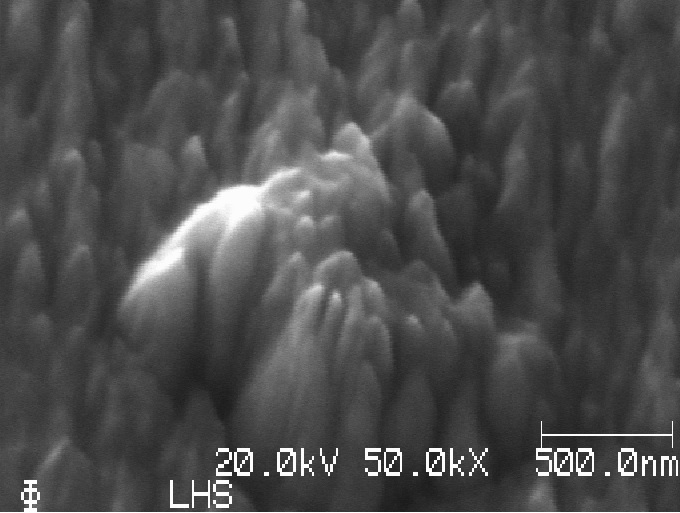
| Equipment: | PHI 680 Scanning Auger Nanoprobe |
| Feature: | A combination of surface sensitive Auger Electron Spectrometer (AES) and high resolution Field Emission Scanning Electron Microscope (FESEM) |
Capabilities
- Nanoscale compositional analysis and imaging (with probe size down to 10nm)
- Large area surface analysis using scan mode
- Elemental Depth profiling with ion sputter gun
- Thin film thickness measurements with calibrated ion sputtering rate Elemental mapping and line scanning
- Dimensional measurement with calibrated scale
Specifications
| Target Signal: | Auger electrons from 5-10nm of the sample topmost surface |
| Elements covered: | All except H & He |
| Detection Limits: | 0.1-1at% depends on element |
| Lateral Resolution: | 10-40nm |
| Image modes: | Secondary Electron (SEM), Auger Electron (Elemental mapping) |
Theory behind
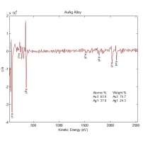
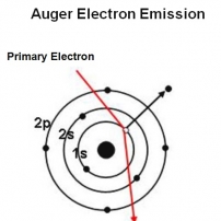
Auger Electron Spectroscopy (AES) is a quantitative analytical technique that utilizes a finely focused high energy electron beam (up to 20keV) as an excitation source to eject Auger electrons from the surfaces of solid materials. The in-situ electron energy analyzer is used to measure the kinetic energy (KE) and number of electrons that escape from the surface. From the kinetic energy and intensity of an Auger peak, the elemental identity and quantity of a detected element can be determined. The average analysis depth of Auger electrons approximately 5 nm which make AES is extremely surface sensitive. The electron beam size is as small as 10 nm which make this technique have very high lateral spatial resolution, high definition elemental line scanning and mapping can be obtained with the scanning function. With equipping ion sputtering gun, elemental distribution against sputter depth (i.e. depth profile) at the surface of a material can be monitored.
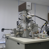
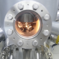
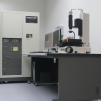
| Equipment: | PHI Quantera Scanning X-ray Microprobe |
| Feature: | A X-ray photoelectron spectrometer with finely focused scanning X-ray probe which could provide not only single point analysis but also imaging and elemental mapping. |
Capabilities
- Surface analysis of organic and inorganic materials, stains, corrosion or discoloration
- Determination of chemical state of the detected elements [e.g, Cu(0), Cu(I) & Cu(II)]
- Elemental and chemical state mapping
- Depth profiling for thin film composition
- Thin film thickness measurements with calibrated ion sputtering rate
Specifications
| Target Signal: | Photoelectrons from 5-10nm of the sample topmost surface |
| Elements covered: | All except H & He |
|
Chemical state information: |
Yes |
| Detection Limits: | 0.1-1at% depends on element |
| Image modes: | Scanning X-ray Induced secondary electron (SXI), Photoelectron (Elemental and Chemical state mapping) |
| Lateral Resolution: | 9 - 200 µm |
Theory behind
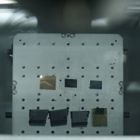
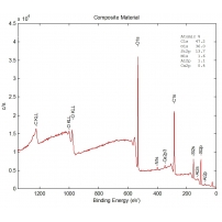
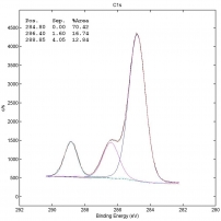
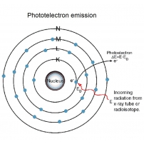
X-ray Photoelectron Spectroscopy (XPS) or Electron Spectroscopy for Chemical Analysis (ESCA) is a quantitative spectroscopic technique that measures the elemental composition and chemical states of the elements that exist in a material. XPS spectra are obtained by irradiating a material with a beam of monochromatic Aluminum X-ray (Al Kα) causing photoelectrons to be emitted from the sample surface. The in-situ electron energy analyzer is used to measure the kinetic energy (KE) and number of electrons that escape from the top 5 nm of the material. From the binding energy (deduced from KE) and intensity of a photoelectron peak, the valuable information about the elemental identity, chemical state and relative amount of the detected elements can then be determined. XPS detects all elements with atomic number (Z) greater than 3, this implies that XPS cannot detect hydrogen (Z=1) and helium (Z=2). With equipping ion sputtering gun, elemental distribution against sputter depth (i.e. depth profile) at the surface of a material can be monitored; the change in chemical state of particular element can also be tracked.
| Equipment: | PHI 680 Scanning Auger Nanoprobe |
Capabilities
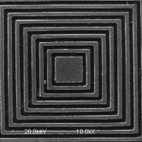
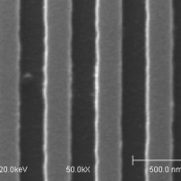
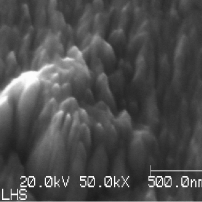
- High magnification image with spatial resolution down to 10nm
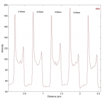
- Dimensional measurement down to submicron level with calibrated scale
Specifications
| Target Signal: | Secondary & backscattered electrons |
| Lateral Resolution: | 10nm at 20kV |
Theory behind
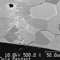
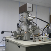
Scanning Electron Microscopy (SEM) is one of the most widely used analytical tools today. It provides high-resolution and long-depth-of-field images of the sample surface that optical microscopy cannot provide. The Secondary Electron (SE) and Backscattering Electron (BSE) images are formed by scanning the sample with a high energy electron beam (up to 20kV). The primary electrons interact with the sample and generate low energy secondary electrons and back-scattered electrons, these electrons are collected by corresponding electron detectors and the surface topography of the sample can be constructed.
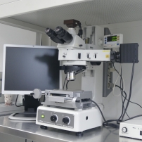
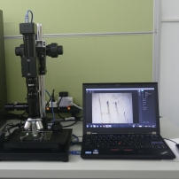
| Equipment: | Nikon MM-400 measuring microscope & SK-HZM digital microscope |
Capabilities
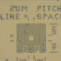
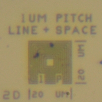
- High magnification color image with spatial resolution down to 1μm
- Dimensional measurement down to micron level with calibrated scale
Specifications
| Target Signal: | Visible light |
| Lateral Resolution: | down to 1μm |
| Image resolution: | 5 Megapixel |
Theory behind
Optical Microscopy is a widely used technique for inspection of surface feature and morphology under visible light with wide range of magnifications; with combination of micro-sectioning, the internal feature of the specimen could also be revealed and inspected. With proper scale calibration, optical microscope can be used for dimension measurement such as plating thickness and particle size.
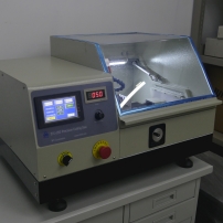
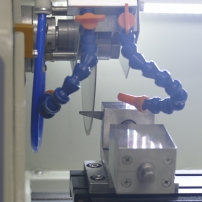
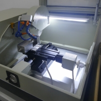
| Equipment: | MTI SYJ-200 precision cutting saw |
Specifications
| Target material: | All types of solid |
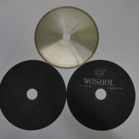
| Blade selection: | Diamond, Silicon Carbide or Aluminum Oxide |
| Feed speed: | 1 -20mm/min |
| Blade speed: | 300-3500 RPM |
| Precision: | 0.01mm |
Description
Precision cutting is a useful sample preparation technique. When sectioning small, delicate, or extremely hard materials, a thin metal bonded diamond blade is used for cutting, the cut piece will have more precise cut, less material loss and less induced deformation than other types of cutting.
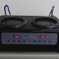
| Equipment: | MTI EQ-Unipol-820 dual platens grinder/polisher |
Specifications
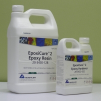
| Mounting medium: | Epoxy resin |
| Grinding tool: | Silicon Carbide abrasive papers |
| Polishing aid: | Diamond or Aluminum Oxide suspension |
| Wheel speed: | 50-600 RPM |
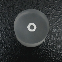
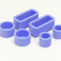
Description
The micro-sectioning is multi-stage sample preparation process for revealing coating layer structure/uniformity, thickness in plating finishes, or ascertaining the internal failure in the bond pad/junction/joint at Printed Circuit Board and electronic packages. The isolated area of interest from the sample is firstly encapsulated into a mounting medium (e.g., epoxy resin) within a mould and is left to solidify. On solidification, the mounted specimen (or micro-section) is subjected to a number of grinding/polishing stages to generate a final polished specimen free of deformation and suitable for optical and/or electron microscopy analysis.